(Hong Kong)

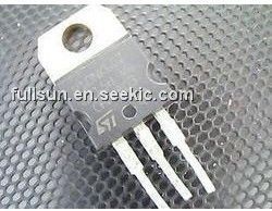
Product Summary
The P5NK100Z is a Power MOSFET which is obtained through an extreme optimization of well established stripbased layout. In addition to pushing on-resistance significantly down, special care is taken to ensure a very good dv/dt capability for the most demanding applications. Applications of the P5NK100Z include Switching application.
Parametrics
P5NK100Z absolute maximum ratings: (1)Drain-source voltage: 1000 V; (2)Gate-source voltage ± 30 V; (3)Gate source ESD: 4000V; (4)Peak diode recovery voltage slope: 4.5 V/ns; (5)Insulation withstand voltage (RMS) from all three leads to external heat sink: 2500V; (6)Operating junction temperature Storage temperature: -55 to 150℃.
Features
P5NK100Z features: (1)Extremely high dv/dt capability; (2)100% avalanche tested; (3)Gate charge minimized; (4)Very low intrinsic capacitances; (5)Very good manufacturing repeatibility.
Diagrams